Invited Speaker

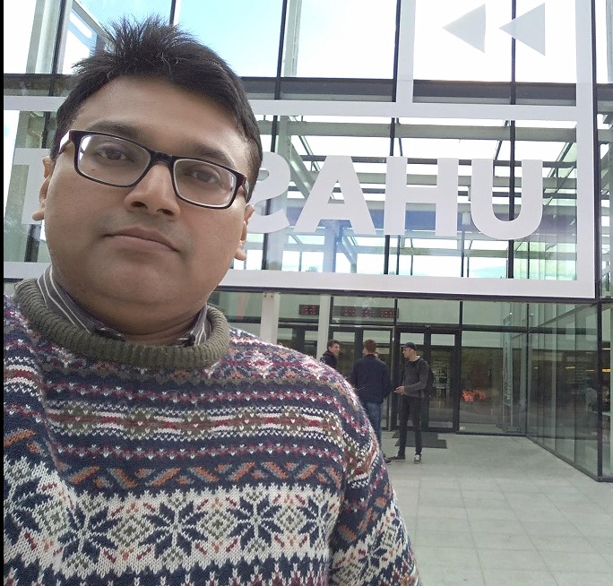
Dr. Awadesh Kumar Mallik
Solvay Business School, Vrije Universiteit Brussel, BelgiumSpeech Title: CVD Diamond – Synthesis, Properties and Applications
Abstract: Unfortunately, the use of classical resonant cavity deposition reactors with the high CVD processing temperature, leads to a decomposition of GaN into elemental Ga and nitrogen gas under the hydrogen plasma CVD diamond growth environment. Here the GaN substrate temperature during deposition is lowered by using innovative linear antenna microwave plasma CVD processing. It was observed that a substrate temperature of around 400 oC could be achieved under a full input MW power of 3 kW, enabling high quality diamond deposition with Raman signal ratio of sp3 diamond to sp2 graphitic content as high as (Id/Ig) 93%. Substrate temperatures beyond 400 oC, could also be reached by employing an additional heater, and further diamond growth was thereby promoted on GaN/Sapphire substrates, leading to a well-facetted nanocrystalline diamond (NCD) film morphology. The successive evaluation of Raman spectra from different NCD on GaN films revealed that the Raman signal for sp3 diamond peak is the most intense one, when pulse mode microwave frequency of 20 kHz at 45% duty cycle was used while keeping the substrate temperature around 320oC. The resistivity of the bare GaN/Sapphire substrate was measured to be 22.2 ohm-cm by Hall four-point probe method. Whereas, NCD coated GaN/sapphire had a higher resistivity of 460 ohm-cm. Linear antenna CVD could successfully deposit nanodiamond films on GaN substrates however by changing the electrical conductivity values significantly.
Keywords: CVD, diamond, GaN, electronics
Biography: Dr. Awadesh Kumar Mallik is an engineer cum scientist, who has been working in the field of CVD diamond materials for the past 20+ years. He has developed processes like hot filament CVD, 915 MHz and 2.45 GHz microwave plasma resonant cavity CVD, linear antenna CVD, Single crystalline CVD for gemstone application, tribology & thermal management by PCD coatings and also fabricated products like diamond discs and foils for MW transmission windows, supporting rods for helix TWTs etc. He has also developed laser cutting and polishing technologies for the as-grown diamond material over large areas with industrial collaboration. Other than working with microwave plasma CVD, he has experiences with industrial cathodic arc PVD of hard nitride coatings, plasma enhanced CVD of diamond like- coatings, MOCVD of alumina coatings etc. In addition to research and development activities, he taught and supervised postgraduate and undergraduate students at the institutes of reputation, like UHasselt, NIT, Rourkela and PESSE, Bangalore. He successfully carried out many international collaborations with different countries.
He also developed expertise in ceramic fabrication techniques like atmospheric sintering, hot iso-static pressurised sintering, laser assisted net shaping, spark plasma sintering, gas pressure sintering, extrusion, slip casting etc. He has in depth knowledge of the different characterisation methods for bulk ceramic samples through his association with ceramic materials over the past 20 years.
He correlates material processing technologies with their observed properties using varied characterization tools, which are well reflected in his almost 40 peer review articles so far. He has organized many international conferences and delivered oral presentations. He relocated to Belgium
for working at the University of Hasselt as FWO postdoctoral researcher in 2018. Currently he is graduating from Solvay Business School, Vrije Universiteit Brussel (VUB), Belgium.

